Original Link: https://www.anandtech.com/show/9825/correcting-a9s-l3-cache
Correcting Apple's A9 SoC L3 Cache Size: A 4MB Victim Cache
by Ryan Smith on November 30, 2015 10:31 AM EST
Along with today’s analysis of Chipworks’ A9X die shot, I’m also going to use this time to revisit Apple’s A9 SoC. Based on some new information from Chipworks and some additional internal test data, I am issuing a correction to our original analysis of Apple’s latest-generation phone SoC.
In our original analysis of the A9, I wrote that the L3 cache was 8MB. This was based upon our initial tests along with Chipworks’ own analysis of the physical layout of the A9, which pointed to an 8MB L3 cache. Specifically, at the time I wrote:
However it’s also worth mentioning that as Apple is using an inclusive style cache here – where all cache data is replicated at the lower levels to allow for quick eviction at the upper levels – then Apple would have needed to increase the L3 cache size by 2MB in the first place just to offset the larger L2 cache. So the “effective” increase in the L3 cache size won’t be quite as great. Otherwise I’m a bit surprised that Apple has been able to pack in what amounts to 6MB more of SRAM on to A9 versus A8 despite the lack of a full manufacturing node’s increase in transistor density.

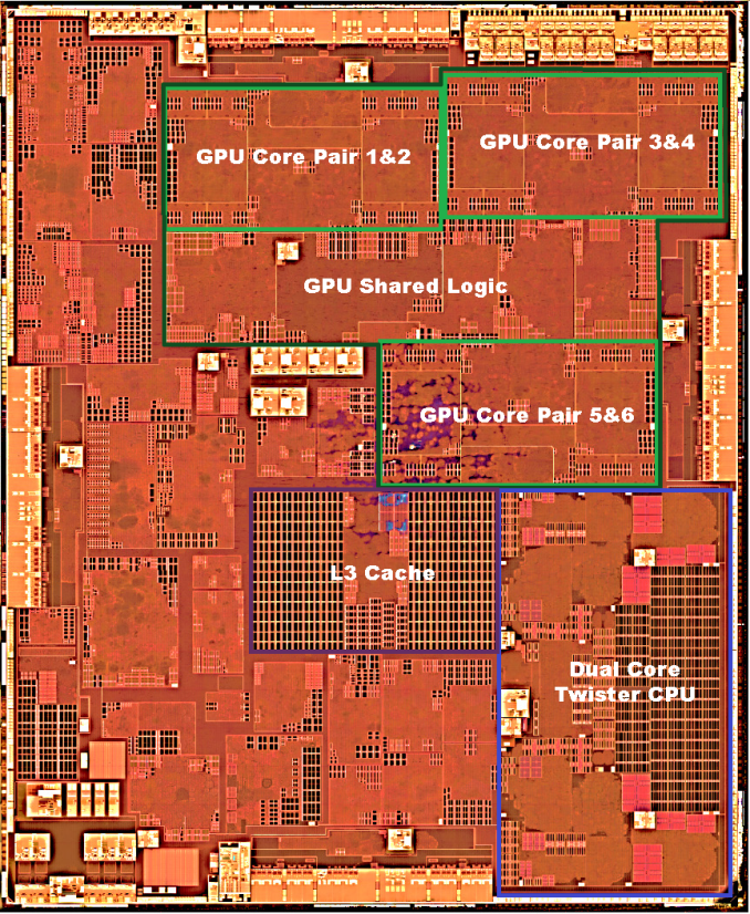
My Layout Analysis For A9 (Die Shot Courtesy Chipworks)
As it turns out, 8MB of cache was too good to be true. After a few enlightening discussions with some other individuals, some further testing, and further discussions with Chipworks, both our performance analysis and their die analysis far more strongly point to a 4MB cache. In particular, Chipworks puts the physical size of the TSMC A9 variant’s L3 cache at ~4.5mm2, versus ~4.9mm2 for A8’s L3 cache. Ultimately TSMC’s 16nm FinFET process is built on top of their 20nm process – the metal pitch size as used by Apple is the same with both processes – and this is the limiting factor for the L3 cache SRAM density.
| Apple SoC Comparison | ||||||
| A9X | A9 | A8 | A7 | |||
| CPU | 2x Twister | 2x Twister | 2x Typhoon | 2x Cyclone | ||
| CPU Clockspeed | 2.26GHz | 1.85GHz | 1.4GHz | 1.3GHz | ||
| GPU | PVR 12 Cluster Series7 | PVR GT7600 | PVR GX6450 | PVR G6430 | ||
| RAM | 4GB LPDDR4 | 2GB LPDDR4 | 1GB LPDDR3 | 1GB LPDDR3 | ||
| Memory Bus Width | 128-bit | 64-bit | 64-bit | 64-bit | ||
| Memory Bandwidth | 51.2GB/sec | 25.6GB/sec | 12.8GB/sec | 12.8GB/sec | ||
| L2 Cache | 3MB | 3MB | 1MB | 1MB | ||
| L3 Cache | None | 4MB (Victim) | 4MB (Inclusive) | 4MB (Inclusive) | ||
| Manufacturing Process | TSMC 16nm FinFET | TSMC 16nm & Samsung 14nm |
TSMC 20nm | Samsung 28nm | ||
But what is perhaps more interesting is what Apple is doing with their 4MB of L3 cache. An inclusive cache needs to be larger than the previous (inner) cache level, as it contains a copy of everything from the previous cache level. On A8 this was a 4:1 ratio, whereas with A9 this is a 4:3 ratio. One could technically still have an inclusive L3 cache with this setup, but the majority of its space would be occupied by the copy of the A9’s now 3MB L2 cache.
So what has Apple done instead? Inlight of Chipworks’ reassessment of the A9’s L3 cache size it’s clear that Apple has re-architected their L3 cache design instead.
What I believe we’re looking at here is that Apple has gone from an inclusive cache on A7 and A8 to a victim cache on A9. A victim cache, in a nutshell, is a type of exclusive catch that is filled (and only filled) by cache lines evicted from the previous cache level. In A9’s case, this means that items evicted from the L2 caches are sent to the L3. This keeps recently used data and instructions that don’t fit in the L2 cache still on-chip, improving performance and saving power versus having to go to main memory, as recently used data is still likely to be needed again.
The shift from an inclusive cache to a victim cache allows the 4MB cache on A9 to still be useful, despite the fact that it’s now only slightly larger than the CPU’s L2 cache. Of course there are tradeoffs here – if you actually need something in the L3, it’s more work to manage moving data between L2 and L3 – but at the same time this allows Apple to retain many of the benefits of a cache without dedicating more space to an overall larger L3 cache.
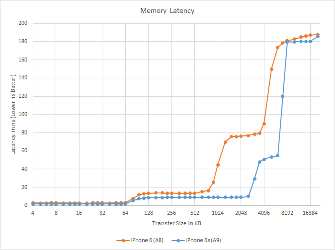
Meanwhile from the software side we can validate that it’s a victim cache by going back to our A9 latency graph. With the exclusive nature of the victim cache, the effective range of the L3 cache on A9 is the first 4MB after the end of the L2 cache; in other words, the L3 cache covers the 3MB to 7MB range in this test. Looking at our results, there’s a significant jump up in latency from 7MB to 8MB. Previously I had believed this to be due to the fact that our testing can’t control everything in the cache – the rest of the OS still needs to run – but in retrospect this fits the data much better, especially when coupled with Chipworks’ further analysis.
Ultimately the fact that Apple made such a significant cache change with A9 is more than I was expecting, but at the same time it’s worth keeping in mind that the L3 cache was only introduced back alongside Cyclone (A7) to begin with. So like several other aspects of Apple’s SoC design, A9 is very much an Intel-style “tock” on the microarchitecture side, with Apple having made significant changes to much more than just the CPU. Though coupled with what we now know about A9X, it does make me wonder whether Apple will keep around the L3 victim cache for A10 and beyond, or if it too will go the way of A9X’s L3 cache and be removed entirely in future generations.


